Making double-sided PCBs using a laser engraver (and a CNC mill) at the Fablab
Project date: January-March 2026
This post is a follow-up to this other post in which we developed a reliable method to make single-sided PCBs by masking boards using acrylic paint, exposing areas of interest using a laser engraver, and etching using ferric chloride.
In principle the process developed up until now is already applicable to both sides of a board, the tricky part in making sure the two sides are aligned. We need some way to register the board: fix it in place and have the machine now where it is exactly. The Workline Model 1290 we have at the FabLab lacks any fixture that could be used to secure the board to the work plane. The first step was to build a jig to do so.
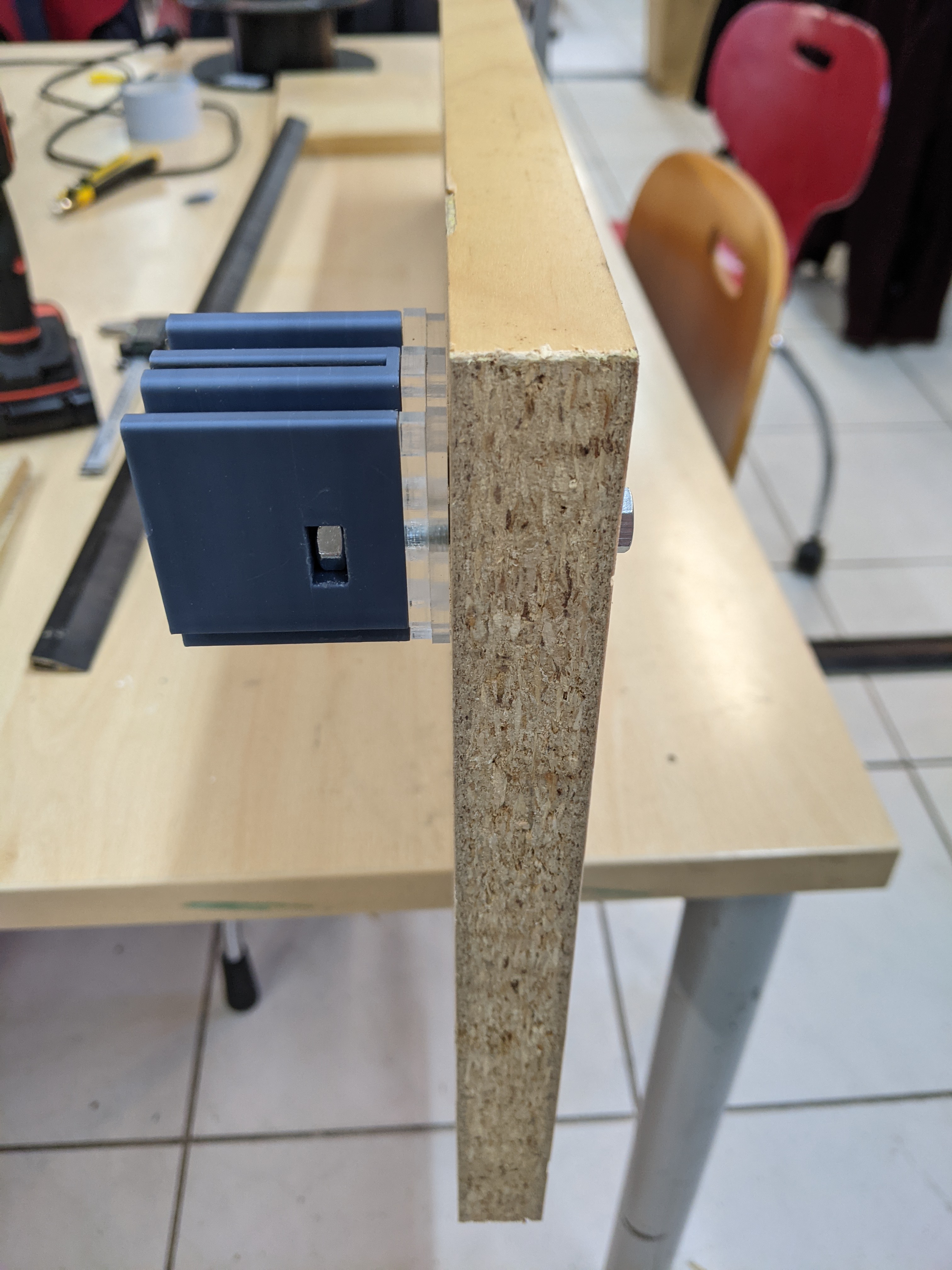
The work plane of the Workline (pardon the accidental alliteration) has this metal bars which fit into groves in the frame and can be removed. I modeled and 3D printed some adapters that could fit into the groves, with holes for a nut though which a wood plank from an old shelf is bolted.
The frame that houses the bars is not even square, so the holes in the plank had to be enlarged and provided some additional degrees of freedom. The bolts were initially kept loose enough to move, but not come apart. Once the board was in position, the bolts were tightened down. The jig is positioned near the origin, where the error the motors should lose very little steps (if none) during long jobs.
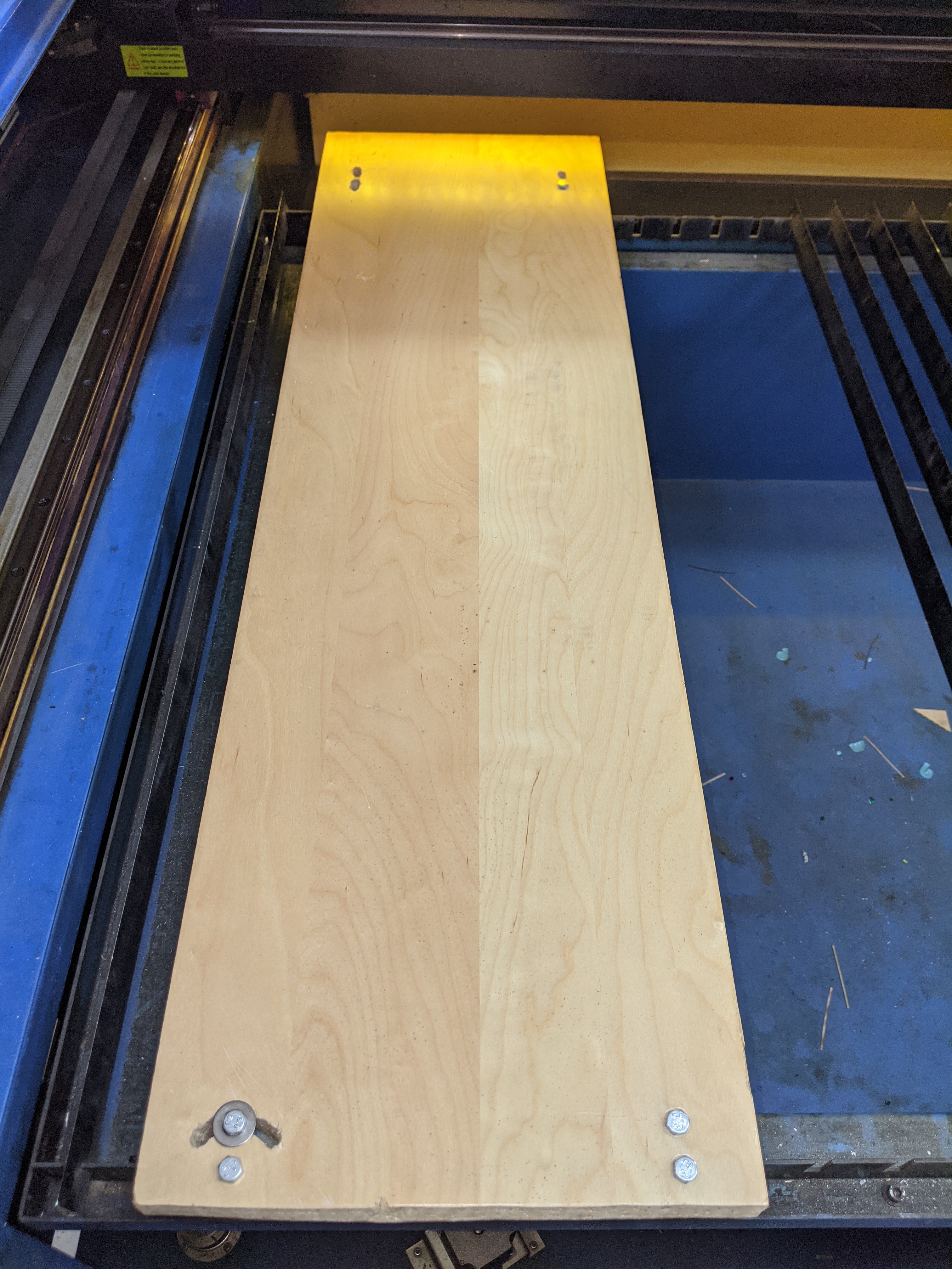
The idea from here was to mark with the laser a known zero point and engrave it on the wood, then use a 3D printed jig to provide alignment to the top-left corner. The jig was actually originally planned to be used on the CNC to make holes for THT components and vias, more on this in a second.
We then proceeded to scrap this idea because we realized that our copper boards were not square, because they were cut manually from larger sheets. Any possible alignment to be done on the laser engraver needs to have a square board.
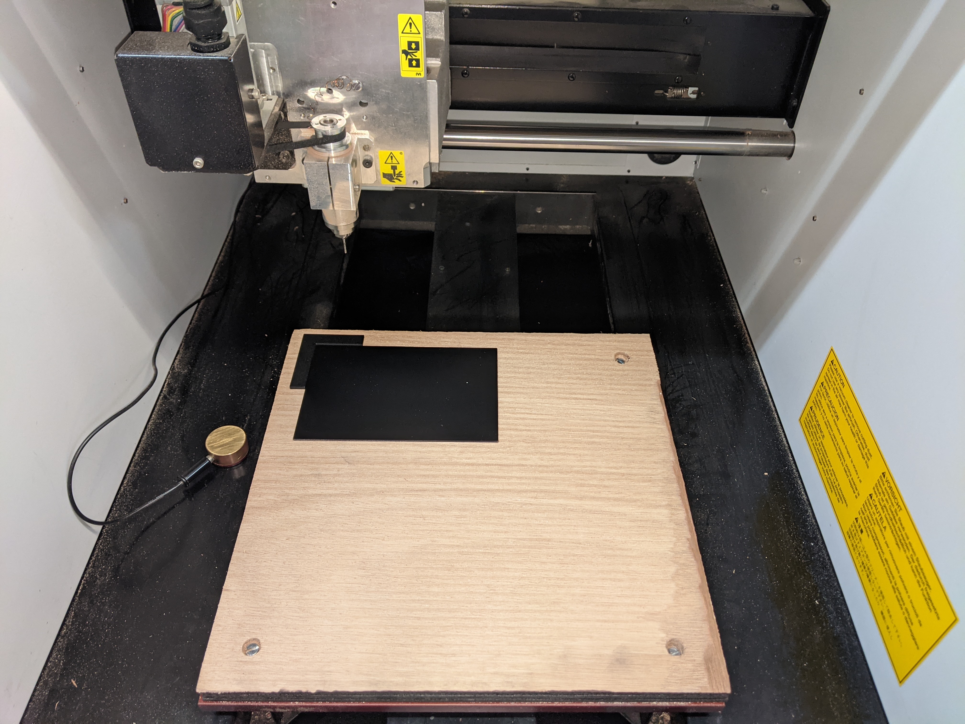
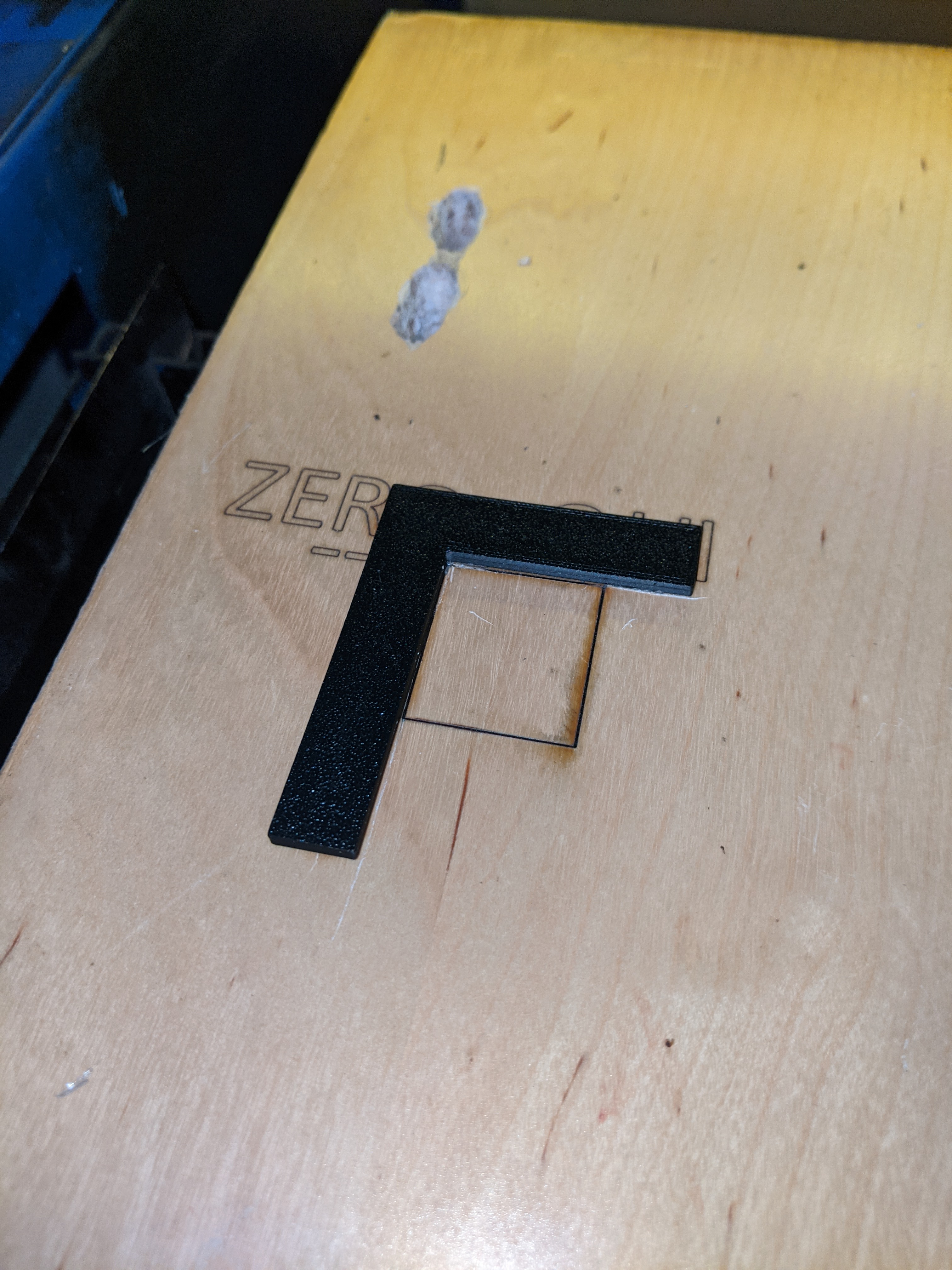
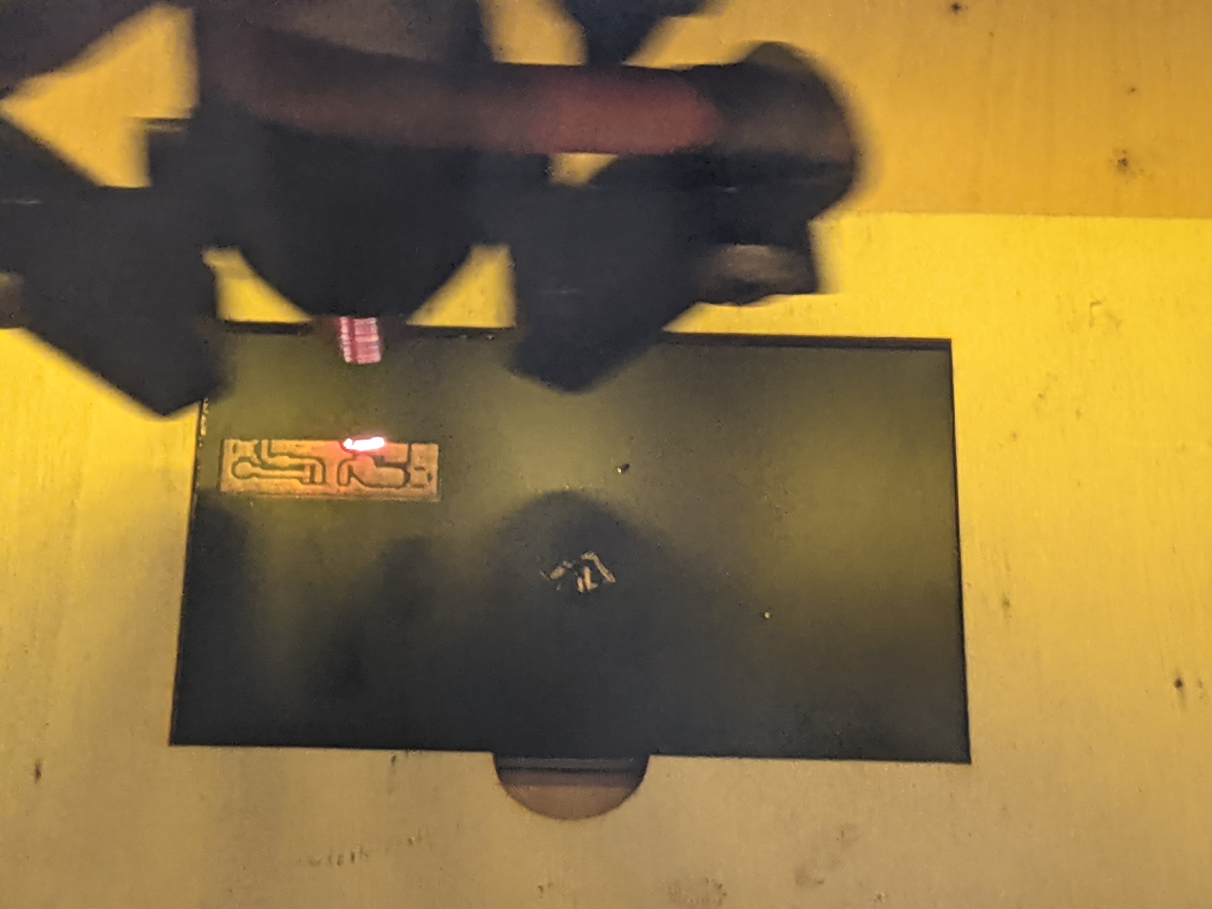
This is where the CNC mill comes in. After securing the board with plenty of double-sided tape, we cut the rectangular contour of the board. The now-square board can be now be moved to be processed on the laser. To register the board, we first tape a sacrificial piece of 3mm plywood to the wood jig, in which we cut the contour of the board. We also add one or more finger holes to easily remove it. After preparation, the board is inserted into the template. From here on, the process goes much like for single-sided PCBs.
With one side finished, the board can be flipped and the second side can be engraved (step 6. of the process is repeated twice, once for each side). Then the process resumes from step 7.
Full process #
-
Import the gerbers into the CNC CAM software.
-
Drill the holes for vias and THT components. I try to lump vias with the smallest THT component I have on the board, so I have to swap bits less time.
-
Cut the contour (Edge_Cuts_ in KiCAD) of the board. We used a titanium coated carbide end mill for this.
-
Follow steps 1-5 of the process for single-sided PCBs:
- Start by thoroughly cleaning the copper with very fine sandpaper to remove any oxide (new: this also removes any residue of drilling holes). The board should be slightly wet to make it easier. I use 800 grit sandpaper.
- Cover the board in degreaser and leave it for about 5-10 minutes, to remove any oil or grease. But make sure NOT to touch the copper with bare hands from now on, to avoid leaving skin oil on the copper
- Clean the board with running water, then dry it with paper or a towel. From now on, when i say “paper”, I mean something like toiler paper or paper towels. It should be soft and able to absorb water.
- Coat the copper side with a thin and even layer of black acrylic spray paint, preferably matte. Shake the bottle for around a minute before coating.
- Wait for the paint to dry, then use some paper to remove any dust that may have deposited on the board meanwhile.
-
Mount the wooden jig the laser. Tape a sacrificial piece of 3mm plywood on it and cut away the contour of the board, along with a hole for easy grabbing. Note that there might be some tolerance to play with when cutting the contour. The cut should be as tight as possible for correct registration.
-
This is analogous to step 6 for single-sided boards. Choose one side of the board, then use the laser engraver to remove the paint from any spot you do not want copper to be on the final board (i.e. anywhere that is not a trace or a pad). Tuning speeds and power depends on your machine, as well as the software used to prepare the machine job. In general this is done by running an engrave job on a DXF file or a black and white image of the copper layer of the PCB.
-
Flip the board and repeat step 6 with the other side of the board. The CAD for this side will need to be flipped as well, in the same away the physical board was flipped (I usually flip both left-to-right).
-
Engraving is done, proceed from step 7 of the original process:
-
Remove the board from the machine, then cover it again with degreaser and leave it for about 5 minutes. Then, clean the board gently with a q-tip or a very soft brush. You should see a greasy patina come away, and then board will appear cleaner since the copper is now actually exposed. Pay attention not to rip away any paint with the q-tip. Also do not use alcohol to clean the board, as it dissolves the paint (IPA in particular). New: repeat this for both sides.
-
Dry the board with paper. DO NOT rub, to avoid removing paint.
-
Etching: Put the board in a bath of Ferric Chloride or equivalent etchant to remove the exposed copper.
- Use protections, like gloves and glasses. Ferric chloride stains the skin and clothes, and cannot be removed. Ask me how I know. If you accidentally splash it on something (including your skin), use wet paper or towel to quickly remove it.
- Use plastic or glass containers for the etchant, metal containers will be corroded just like the copper on the board.
- You can use some long strips of adhesive to maneuver the board, just make sure not to cover the portion you are etching with the tape.
- The time needed and the final product will depend on a number of factors: ferric chloride likes to be warm (I use about 50°C) and stirred. If done well, etching should take about 10 minutes. On the other hand, it took me more than a hour to etch one of the test squares with a cold (20°C) and not stirred etchant.
- I use my old Anet A8 3D printer (bed slinger, with a moving Y axis) to do the warming and stirring. I used gcodepy to create a gcode that warms the bed to 50°C, moves the extruder out of the way and makes the bed move back and forth following a sine wave for stirring.
- Do not leave the board in acid too long, or even the areas with paint on top will become exposed and will be etched away (underetching)
-
When done, remove the board from the acid bath, and use slightly wet paper to remove any residue.
-
Use acetone to remove the remaining paint from the board, exposing pads and traces. New: repeat this for both sides.
-
Cut your PCB to size, removing excess margins. I use the back side of a Stanley knife to define the cut on the board, the snap it using the side of a table.
-
We’re done! Congrats!
-
CAD, CAM, and job preparation #
In KiCAD, I export three layers as DXF: Edge_Cuts, F_Cu and B_Cu. I then import all three into Inkscape to produce DXF for the laser. I duplicate Edge_Cuts, then select all paths and align them all to the center. I also resize the sheet to the selection (CTRL+Shift+R). I group one Edge_Cuts and F_Cu, then group the other Edge_Cuts and B_Cu. I select the second group (the one with B_Cu) and flip it horizontally. I finally export the two groups separately as DXF, and import them into the laser’s CAM.
This process can also be adapted to produce panels, by creating an outer larger rectangle containing all boards (Edge_Cuts can still be mantained to separate individual boards), both for the front and for the back, then flipping the back panel, with respect to the outer rectangle.
The laser’s CAM has a ton of quirks, but the main take away is that I fix the origin on the laser controller itself, and then use Edge_Cuts to cut the contour into the sacrificial plywood, as well as cut the finger hole. In our CAM, the origin of the cut is always computed with respect to the larger closed rectangle, which in this case should be Edge_Cuts and should not change for any reason when changing between the front and the back sides of the board.
We decided to use FlatCAM for CAM on the CNC side. While we are at it, we can also take the time to swap bits and drill holes for THT components and vias. From KiCAD, I export a gerber for Edge_Cuts, one for THT holes, and one for non-THT holes (mounting holes, vias). To ensure consistency with the registration on the laser, I select them all and center them to the origin (doing this is a bit finnicky, the most important thing to note is that to choose the center well, Edge_Cuts must be selected and used as reference). I am really not the best person to talk about CNC jobs, as I have only recently started to learn how to use them for the sole purpose of making PCBs. I referred to this list of tutorials for version 8.991 BETA of FlatCAM.
A side-note for using FlatCAM on linux: FlatCAM is a very old (and seemingly unmaintained) software. A native version for linux can be compiled from source, but some libraries may be too old to be found easily packaged in modern distros. I had a much easier time using the windows version through wine.
Vias #
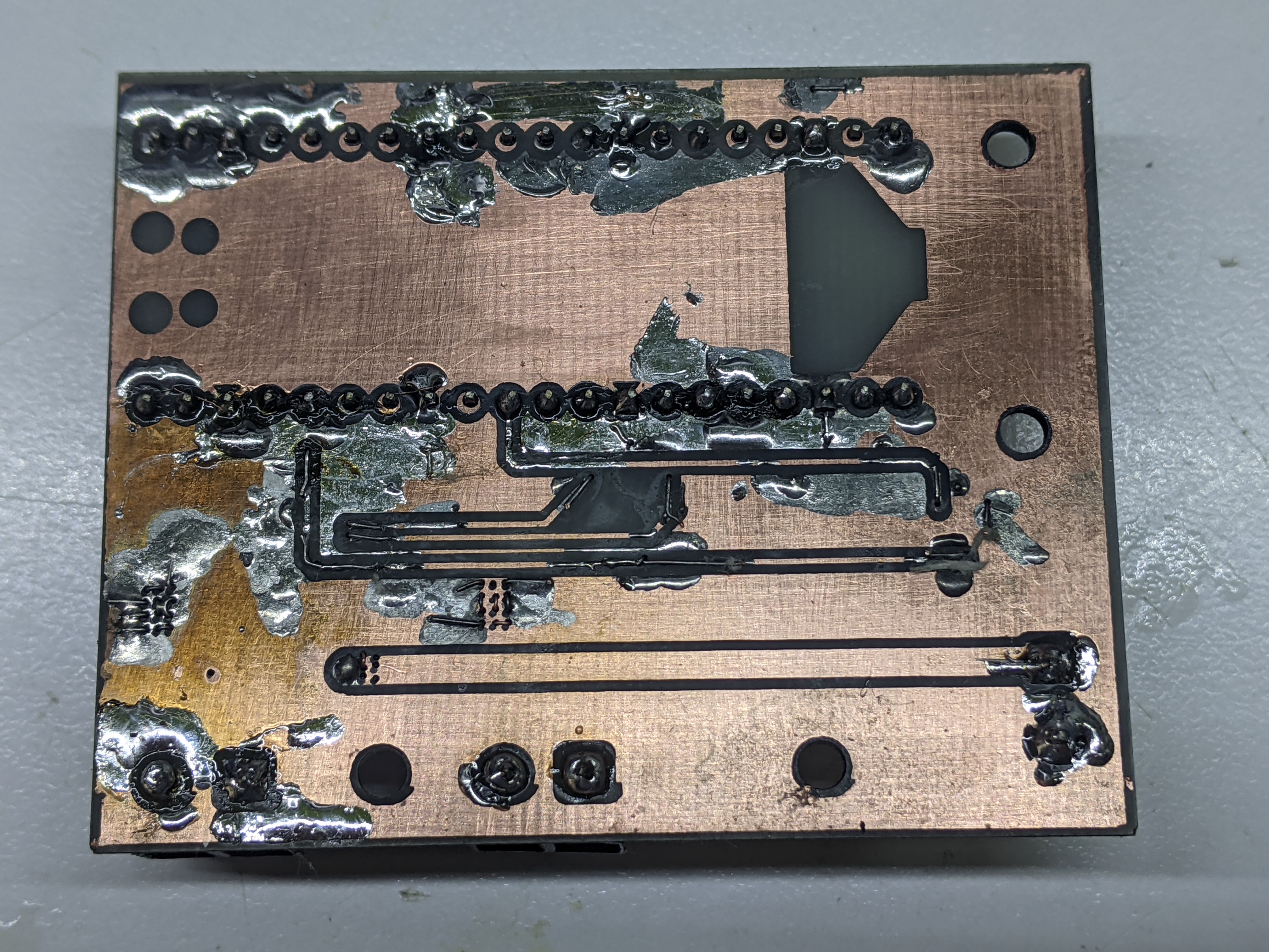
In industrially produced PCBs, the interior of vias is plated with copper to connect the two layers. This mostly involves nasty chemicals I’d rather not deal with, and is not practical on the small scale I need. An alternative is using some special copper rivets, but I haven’t seen any with an outer diameter smaller than 0.8mm. The next best thing is to just weave some stripped 28 AWG wire through 0.3mm or 0.4mm holes and solder it on both sides of the trace/plane, see the PCBs below.
Finished product #
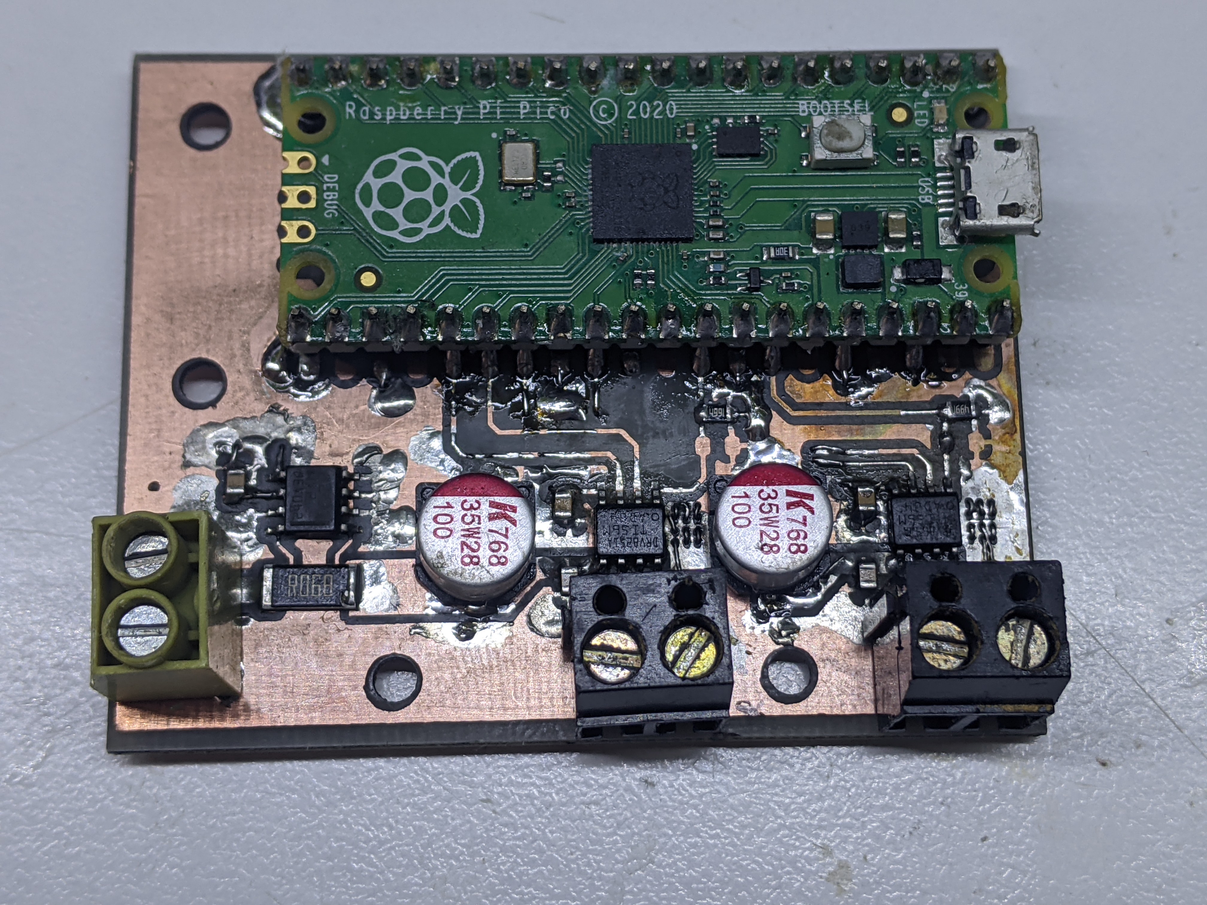
For another project of mine I developed PCBs for the DRV8231 motor driver, with an INA240A3 current sensor as well. I then upgraded the PCB to have a Pi Pico as well to do closed loop torque control of a Brushed DC motor.
The first gallery of images is the production of a smaller PCB with just the motor driver and the current sensor. They turned out quite well. The two sides were perfectly registered, which could be easily seen by shining a light through the PCB and observing that around pads for THT components there was no shadow of the pad on the other side. Holes were a bit misaligned.
In both PCBs, the slight copper contour around the board is actually a workaround to our laser’s CAM, as it does not allow to negate an engrave. Without the added contour, all traces would be removed and only the space in between would be kept.
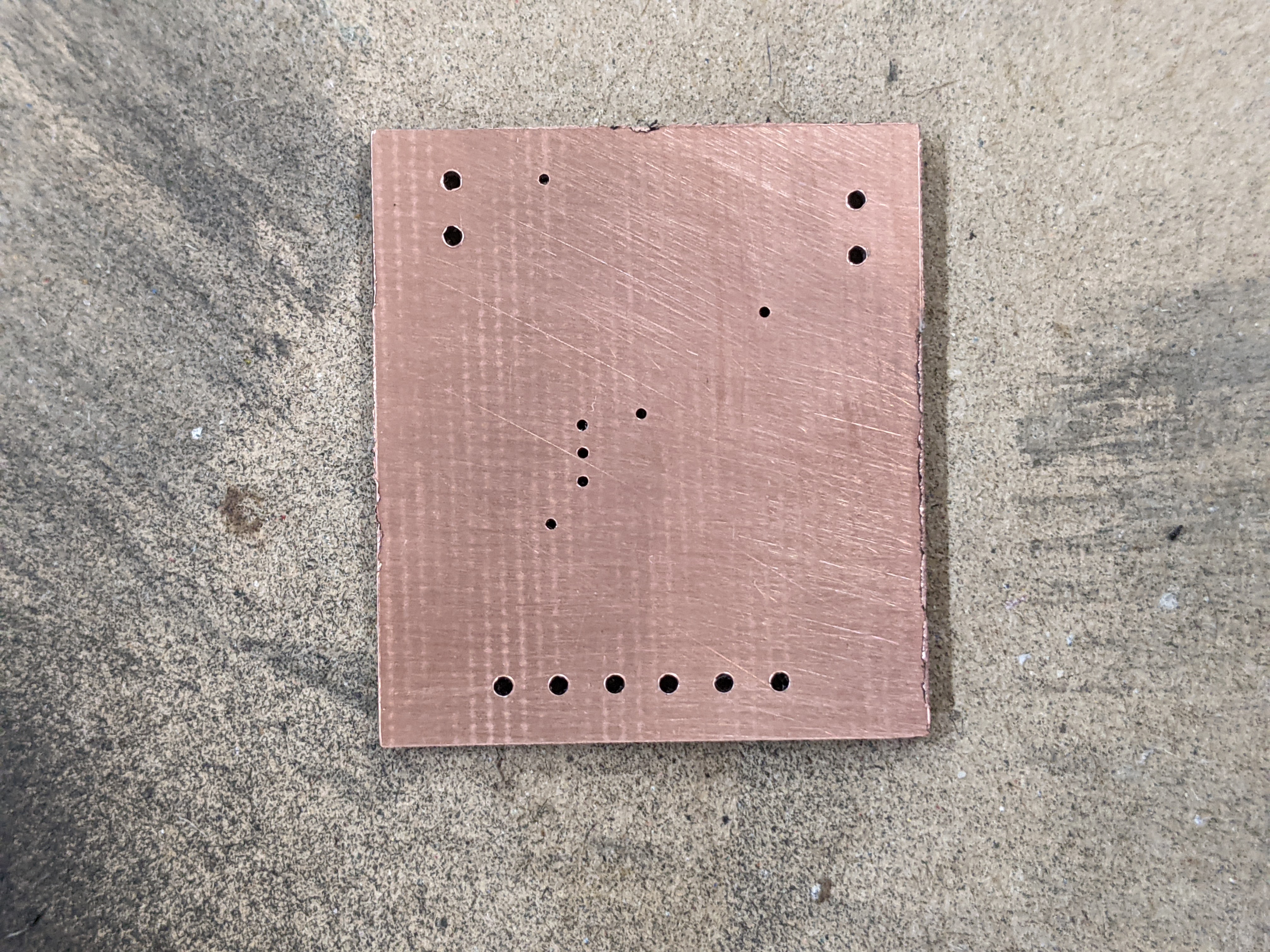
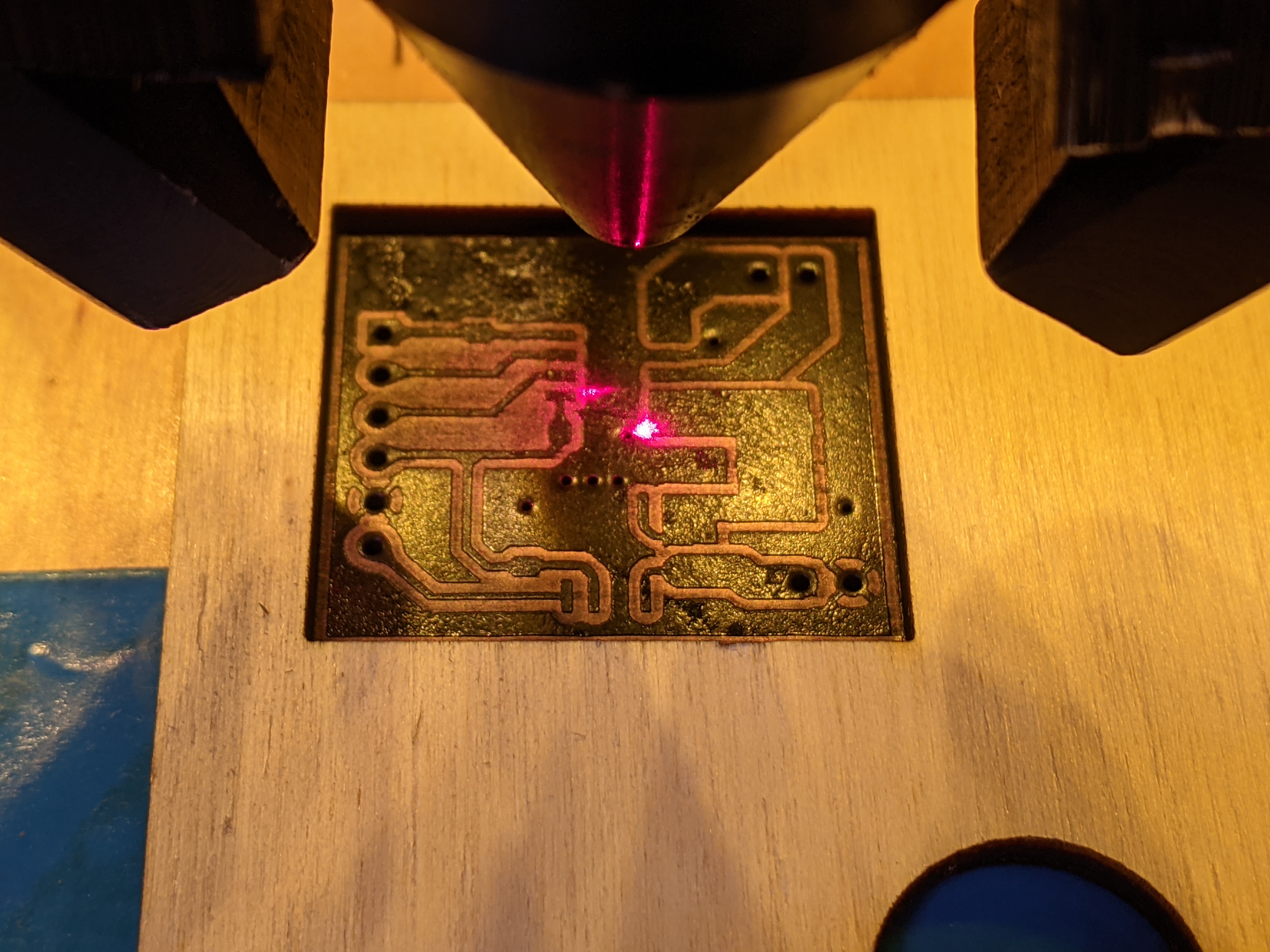
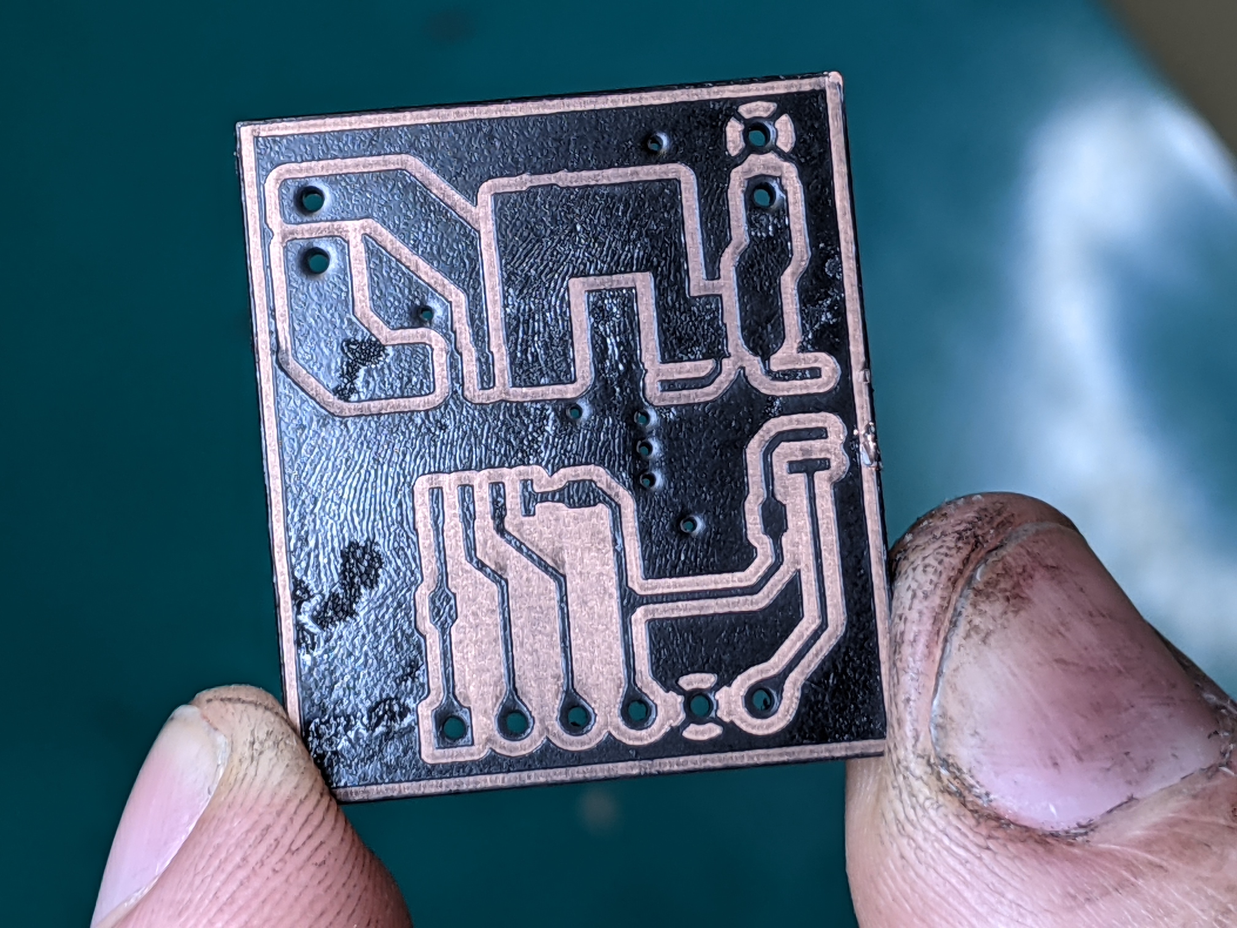
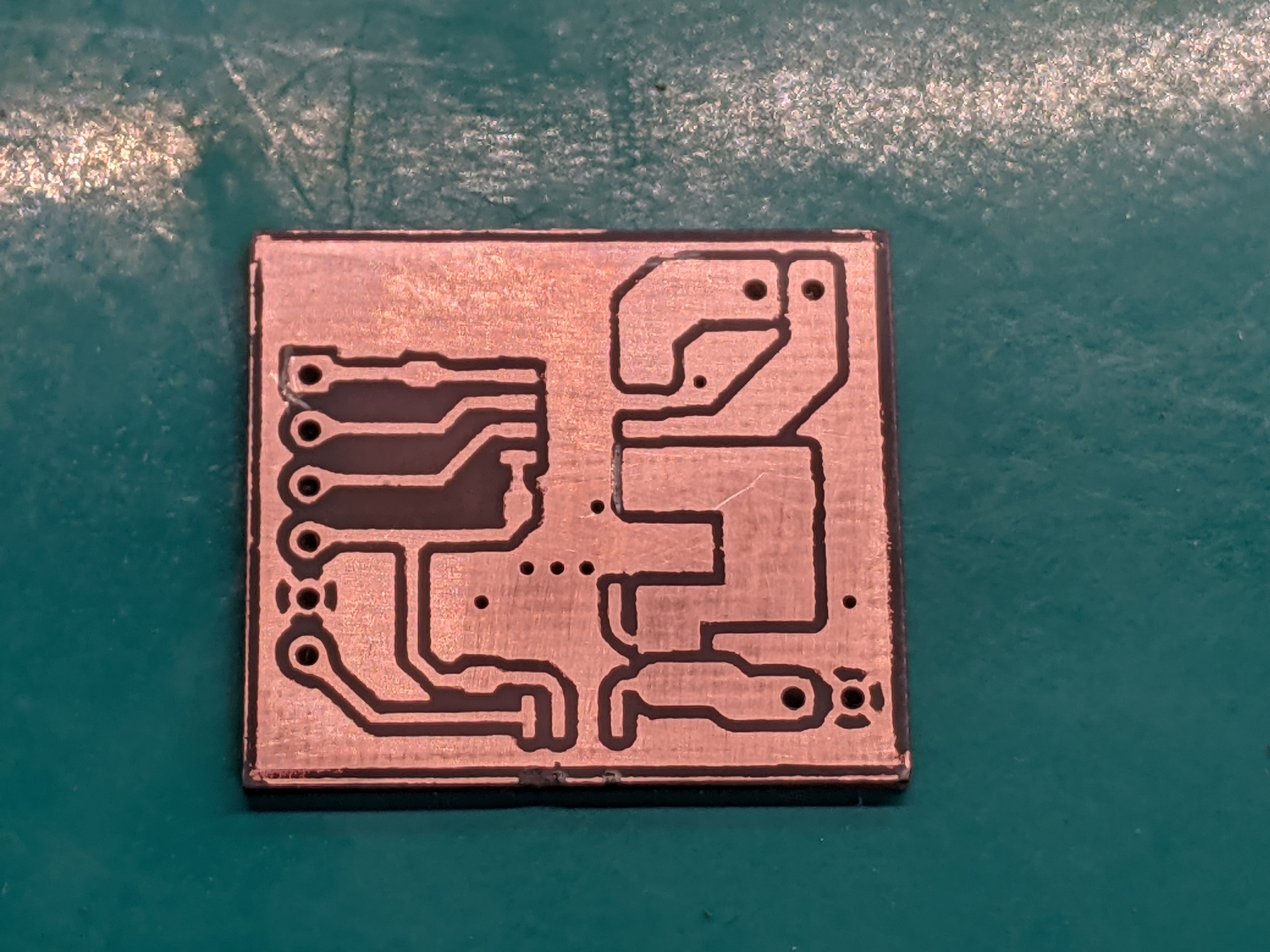
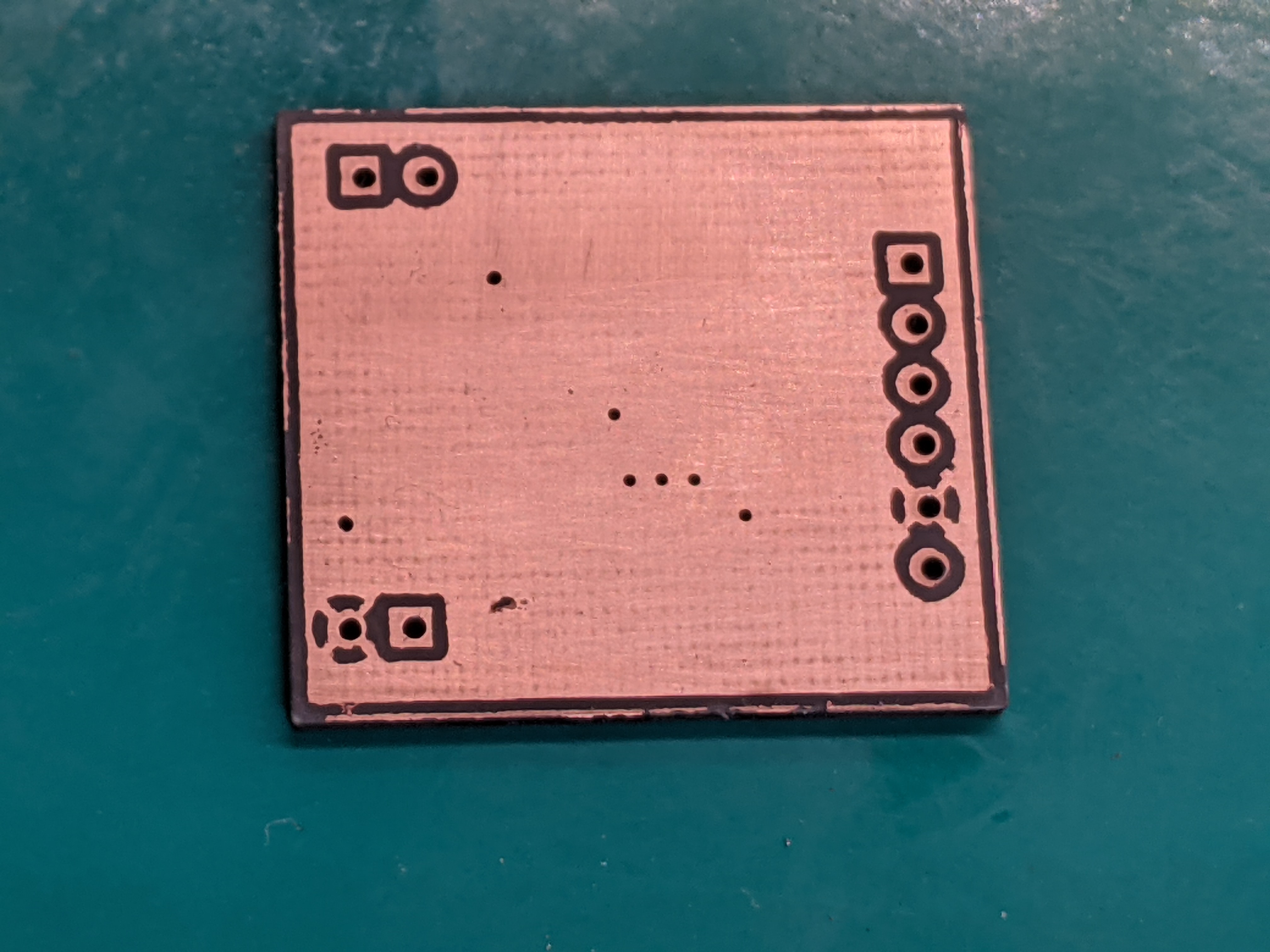
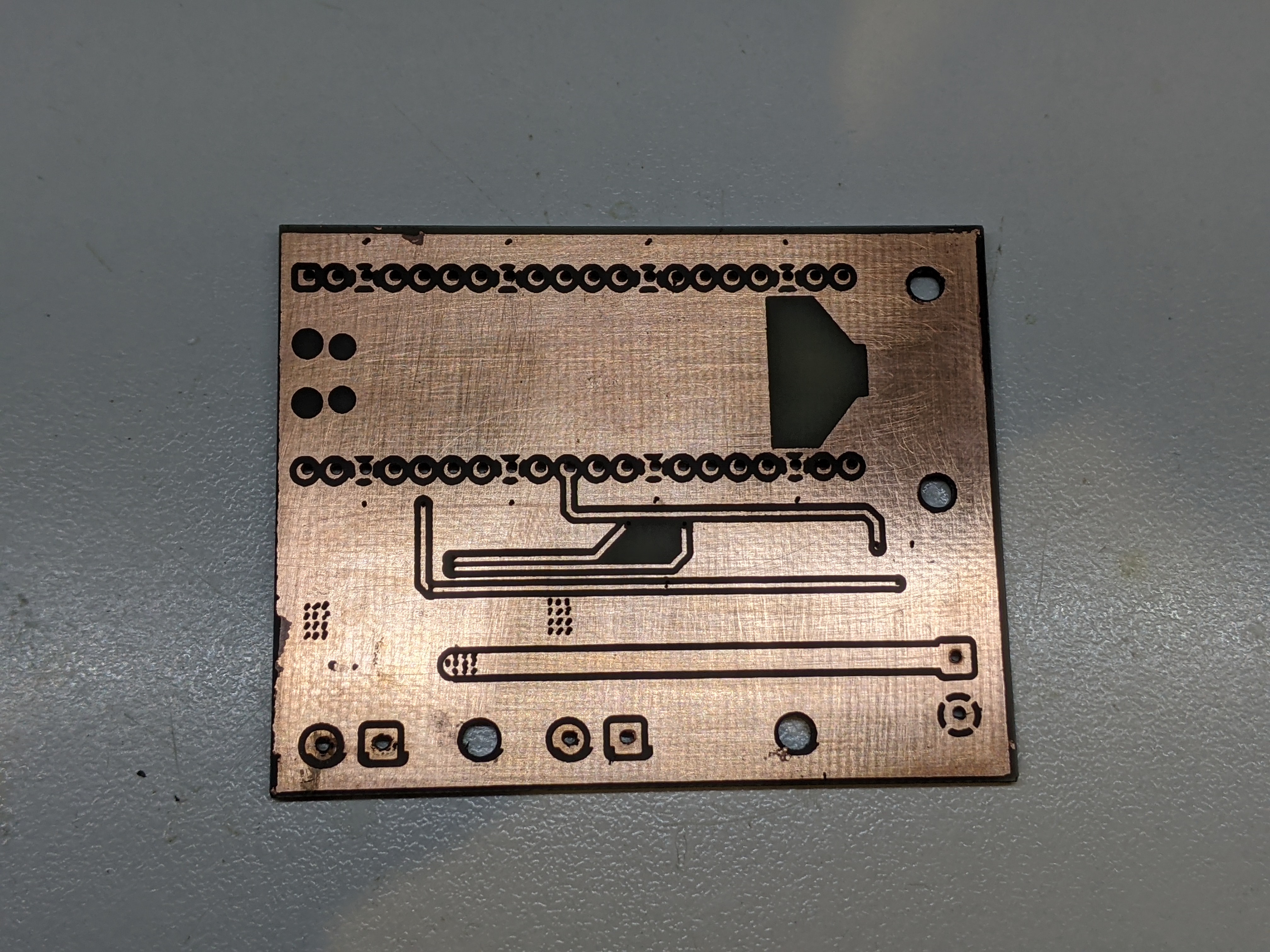
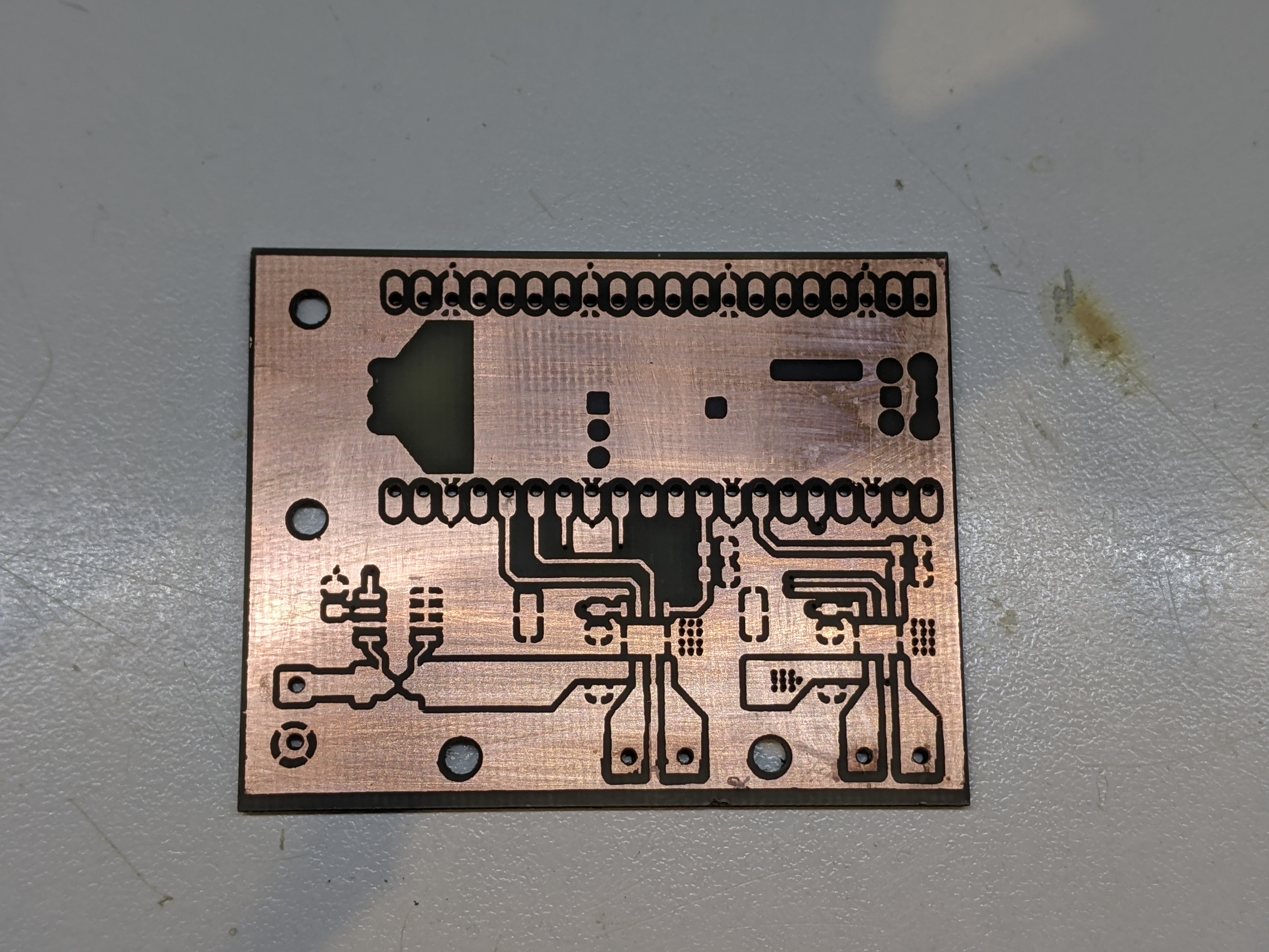
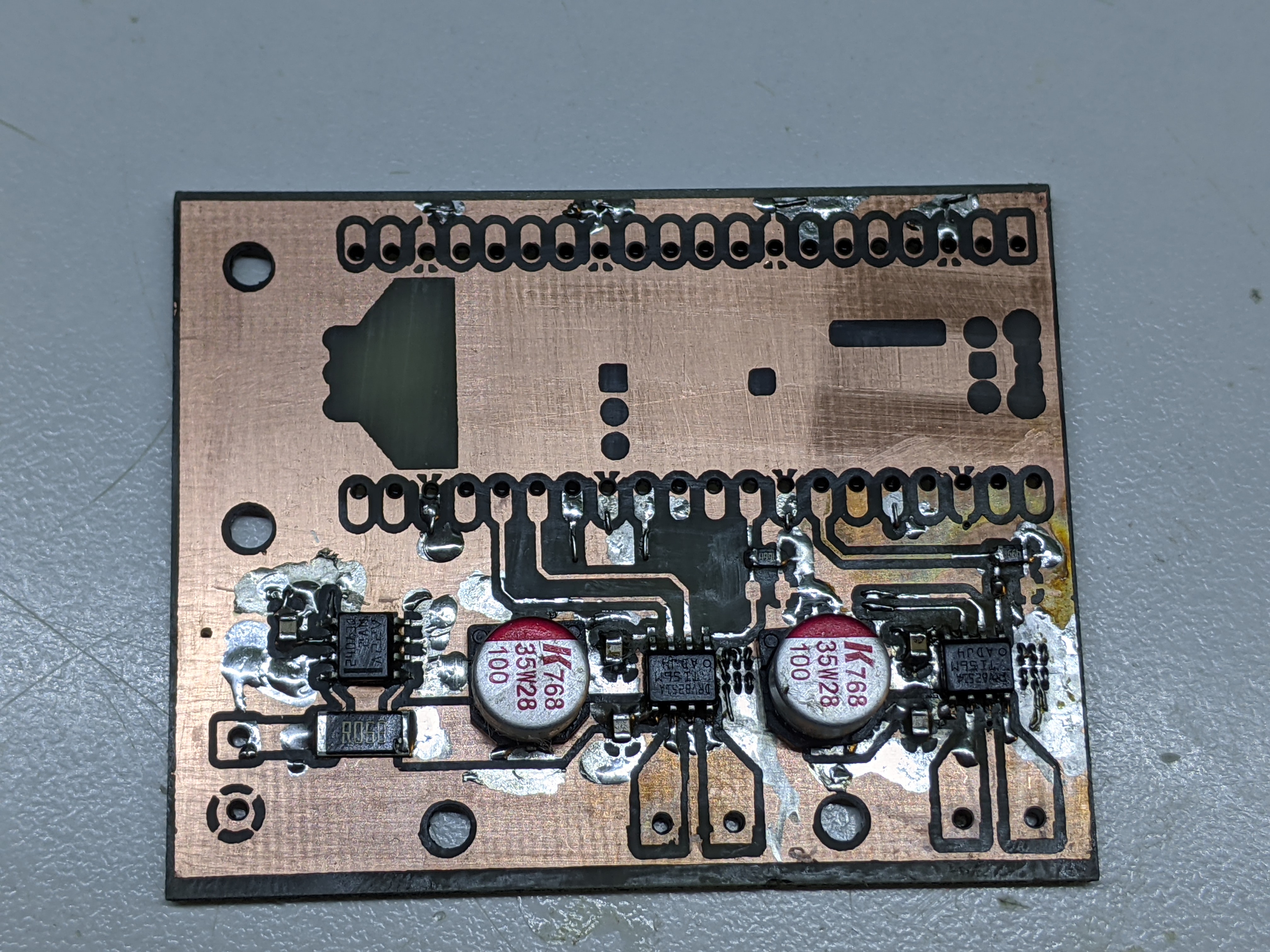
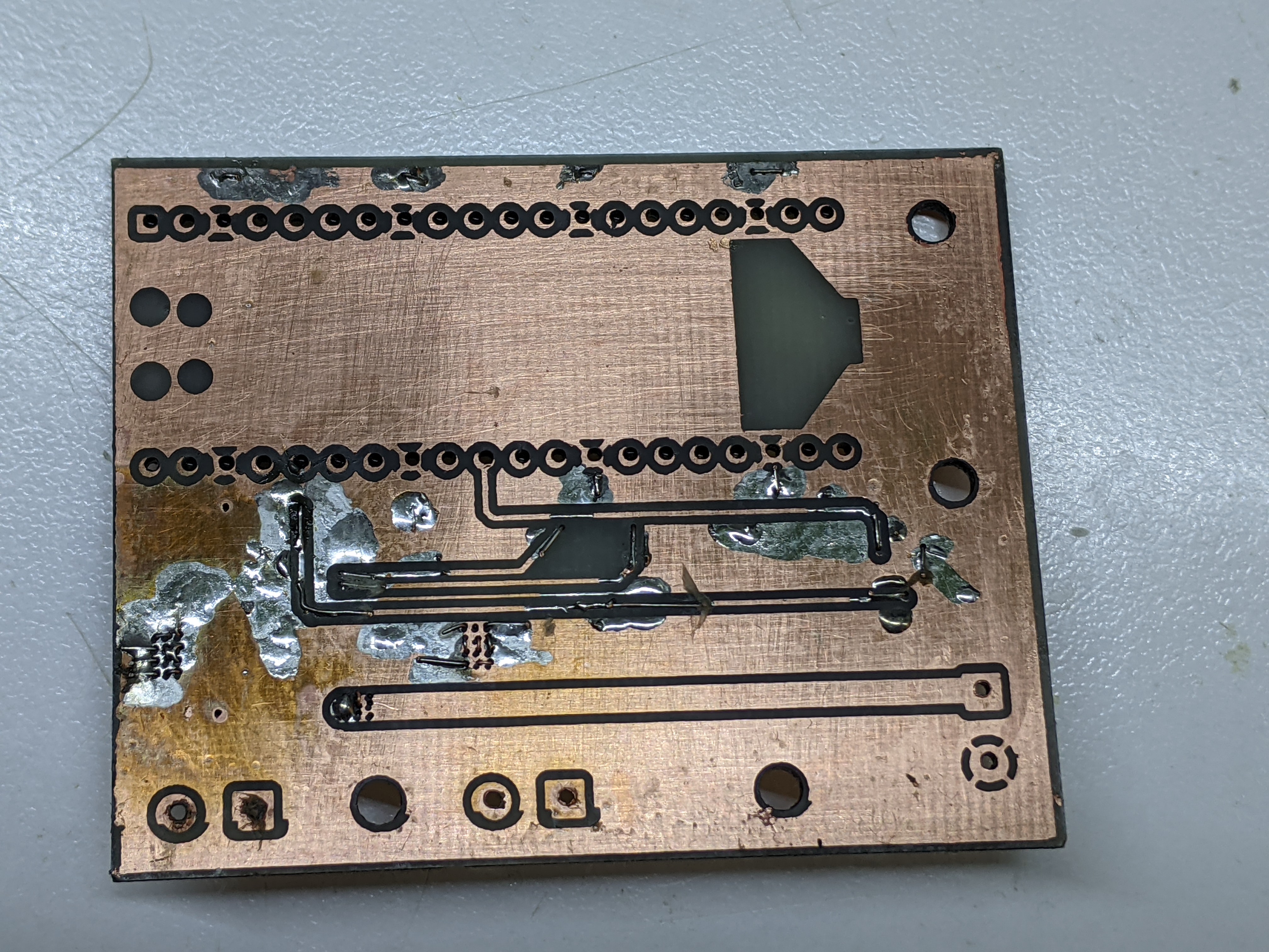
The second gallery of images is the full board with the microcontroller. Vias can also be seen. Holes are more misaligned than in the first PCB, and I later diagnosed this problem with incorrect alignment to the center in FlatCAM. If you zoom in, you can see how vias were connected with stripped wire.
Soldering is a bit of a mess as, without a silkscreen, solder tends to go everywhere.
Soldering the microcontroller was also a bit of a pain, as I tried to use the THT components itself to connect the two layers. This meant that the microcontroller is kept slightly higher than normal, and is soldered on both sides. I didn’t solder unused pins of the microcontroller in case I needed to desolder it later (I did).